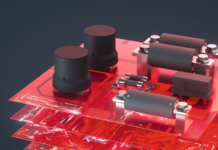
When creating electronic devices, the design of PCB (Printed Circuit Board) is extremely important. It is crucial to check and understand the design before making the actual board to avoid problems during manufacturing. In the PCB design world, Gerber files are a standard way to show the different layers of PCB. NextPCB features a Free Online Gerber Viewer that makes it easy to see and inspect these files. This article will discuss the features and benefits of NextPCB’s Gerber Viewer and how it makes designing PCBs easier.
A Detailed Overview of NextPCB’s Free Online Gerber Viewer:
NextPCB has a cool web-based tool called Free Online Gerber Viewer that can be used on the Internet. It is designed for designers to check out Gerber files, which are like blueprints for PCBs. The viewer allows you to see different layers, including copper, solder mask, silkscreen, and drill holes so that designers can see the whole picture of their PCB design.
Unveiling Its Key Features and Advantages:
Hassle-Free File Upload: Uploading Gerber files is a breeze with Gerber Viewer. All you need to do is just drag and drop the files onto the viewer’s interface, and it will show the PCB design right away.
Controlling PCB Layers Efficiently: With NextPCBs Free online Gerber Viewer, you have control over layers. This way you have control over which layers to see and which ones to hide. This makes it easier for designers to look closely at the PC layout.
Dynamic 3D Display: Using Gerber Viewer, you can see the PCB design in 3D, which makes it look more like a real thing. This helps the designers to check the design from all angles, and find problems like parts that might be blocking each other or are too tall.
Precise Zoom and Measurement: To study the PCB design in detail designers can use zoom and measurement tools with NextPCB’s Gerber Viewer. It helps to measure things precisely, like where the components are placed, trace widths, and distance between parts.
Hands-On Gerber Editing: NextPCB free online Gerber Viewer allows designers to put notes right on the PCB design. This interactive editing feature helps the team members to seamlessly collaborate and communicate. Moreover, they can share comments and feedback within the viewer.
Seamless Compatibility and Cross-Platform Access: The Gerber Viewer works on the web, so there is no need to install the software or worry about compatibility. One of the best benefits for users on the go is that they can use it anytime and anywhere with access to the internet. Also, this makes it perfect for designers working on different platforms and in different locations.
Wrapping Up: Key Takeaways
NextPCB’s Free Online Gerber Viewer is a valuable tool for PCB designers. It has a lot of notable features that help designers check and verify their designs during the process. The Viewer has an easy-to-use interface, lets you control the layers, presents a 3D visual, and has zoom and measurement tools. You can even edit the design interactively. With all these handy features, designers can find and fix any problems before making the actual circuit board, resulting in saving time and money.
Whether you are a pro PCB designer or just do it for fun, NextPCB’s Gerber Viewer makes inspecting and working together easy, helping you create top-notch PCBs. Try this free online tool and open the gates for new chances in your PCB design journey.
FAQ:
What is a Gerber file?
Why do PCB designers need a Gerber viewer?
What advantages does NextPCB’s Free Online Gerber Viewer offer?
Seamless uploads: Designers can quickly upload their Gerber files by dragging and dropping them to the viewer.
Efficient Control on Layer and Visibility: Users can show or hide specific layers to focus on specific aspects.
3D visualization: To allow the designer to analyze the design from all angles and identify the problem, the Gerber Viewer provides a 3D view of the PCB design.
Zoom and measurement Capabilities: Designers can zoom in and out at various magnification levels for the perfect measurements.
Interactive Gerber editing: Users can add comments and notes directly on the PCB design. It also allows the team to collaborate and communicate easily.
Cross-platform access:
This web-based tool can be accessed from any device, requiring only an internet connection. It eliminates compatibility concerns, making it easy to access across different platforms.


